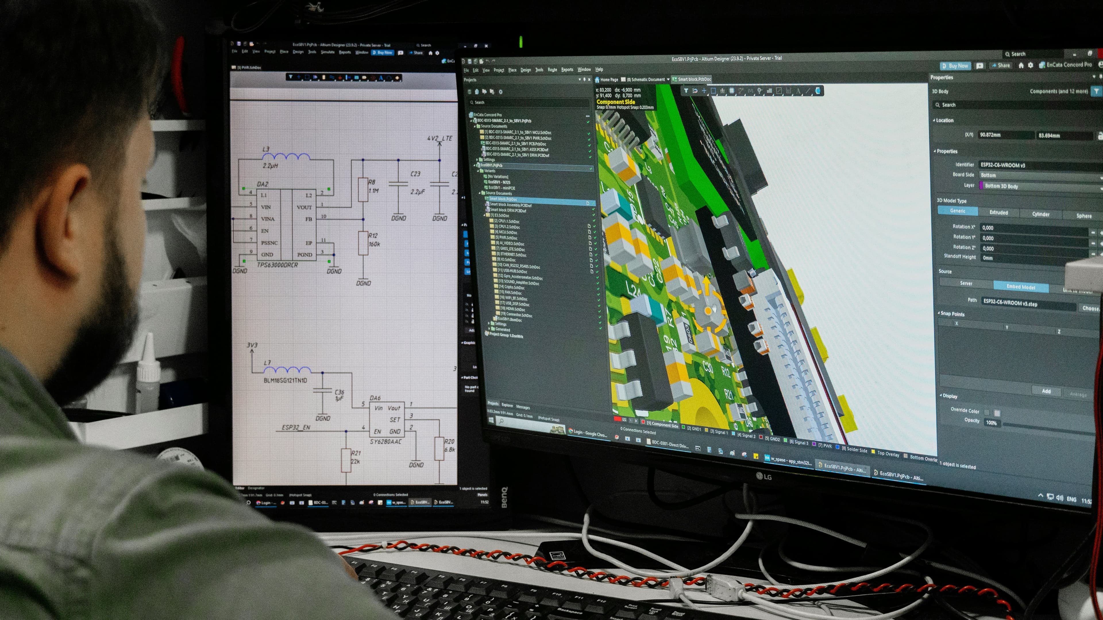
Custom PCB Design
Built for Production
Electronics Circuit & PCB Design
Custom circuit design and multi-layer PCB layout engineered for reliability, signal integrity, and production scale.
Our Approach
#At Kabani Tech, every PCB we design is built for production — not just the prototype bench. Our hardware engineers carry designs from schematic capture through multi-layer layout, signal integrity analysis, and DFM review, producing boards that work reliably from the first build.
We work across power electronics, mixed-signal, RF, and high-speed digital designs. Whether you need a compact wearable PCB or a complex industrial control board, our team handles the full hardware design lifecycle.
Services We Offer
Schematic Design
Detailed schematic capture with component selection, power architecture, and interface definition.
Of PCB failures originate from schematic-level errors caught too late.
62%PCB Layout
Multi-layer PCB layout optimised for signal integrity, thermal performance, and EMC.
First-pass PCB success rate with our layout and pre-compliance process.
91%Signal Integrity Analysis
Simulation and analysis to verify signal quality before the board goes to fabrication.
Reduction in costly PCB respins with pre-fabrication signal integrity checks.
3xDFM Review
Manufacturing readiness review to eliminate fabrication and assembly issues before files are released.
Of PCB assembly issues are avoidable with a thorough DFM review.
75%PROCESS
Our step-by-step custom process
First, we audit your brand and goals. You get full transparency, fast turnarounds, and results that speak for themselves.
Requirements & Schematic Capture
Design requirements agreed, components selected, and schematic created with formal peer review.
PCB Layout
Layer stack-up defined, placement performed, routing completed with DRC passing.
Signal Integrity & Pre-Compliance
Simulations run and layout adjusted to meet signal quality and EMC targets.
DFM & Fabrication Release
Full manufacturing package generated, DFM review completed, and files released to fabrication.
Industries We Serve
We design and engineer digital solutions for high-impact industries.


Frequently Asked
Short on time?
Let's get started with a brief intro call.
What EDA tools do you use?
We primarily use Altium Designer. We can also work in KiCad and deliver in Eagle format on request.
Do you manage PCB fabrication and assembly?
Yes. We can manage the full supply chain from gerber release to assembled and tested boards delivered to your door.
Can you redesign an existing PCB?
Absolutely. We regularly take existing board files and redesign for cost, size, performance, or component obsolescence.
What layer counts do you design to?
We design from 2-layer up to 16-layer boards, with impedance-controlled stack-ups for high-speed and RF applications.

Related Services
Explore other ways we can help you innovate and grow.
Embedded Firmware Development
Low-level firmware that makes your hardware perform — reliable, efficient, and production-ready from the start.
System Architecture Design
A unified technical blueprint that aligns hardware, firmware, and software before a single component is ordered.
Rapid Prototyping
From concept to functional prototype in the shortest possible time — so you can validate, iterate, and move forward.